Transistor-Level MAC Datapath & SRAM Design
Fri Dec 12 2025
Overview
This project is a full custom, transistor-level MAC datapath with integrated SRAM, built for ECE 467 Introduction to VLSI during my first semester in the MS ECE program at UIC.
Everything was designed directly in Cadence Virtuoso at the schematic level. Logic gates, arithmetic blocks, memory cells, decoders, and buffers were all built from transistor primitives, simulated, and then composed into a complete working system.
The goal wasn’t performance tuning or optimization - it was learning how real full-custom CMOS design actually works: building systems bottom-up, validating them through simulation, and integrating logic, memory, and datapath structures into a real architecture.
System Structure
At a high level, the system is made up of several independently designed blocks that were later integrated into a single datapath:
- Custom transistor-level logic gate library
- Arithmetic blocks (adders + multiplier)
- SRAM memory structures
- Decoder and control logic
- Signal routing and buffering circuits
Each block was designed, simulated, and verified on its own before being hierarchically integrated into the full system.
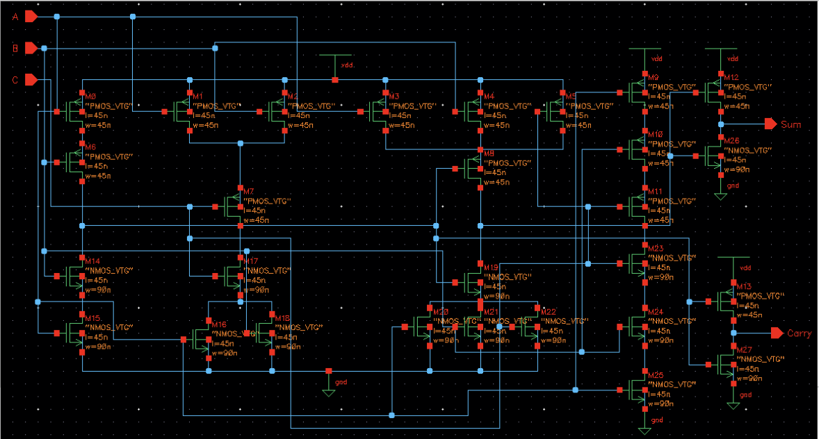
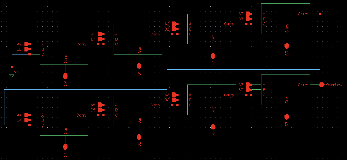
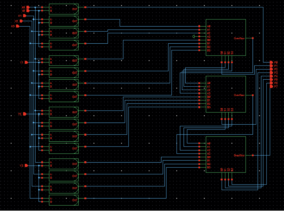
MAC Datapath
The MAC datapath is built from reusable transistor-level building blocks that form a simple arithmetic pipeline.
It is composed of:
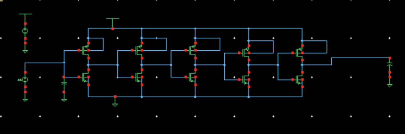
- a custom 1-bit full adder cell as the base primitive
- an 8-bit adder built hierarchically from those cells
- a 4-bit multiplier integrated into the accumulation path
All arithmetic structures were implemented directly at the transistor level and validated through schematic-level simulation.
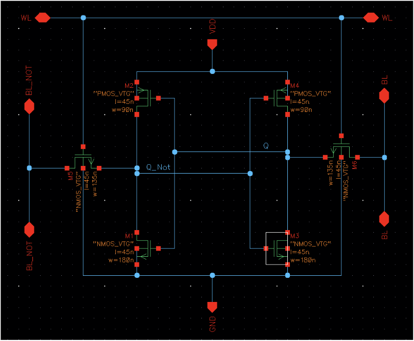
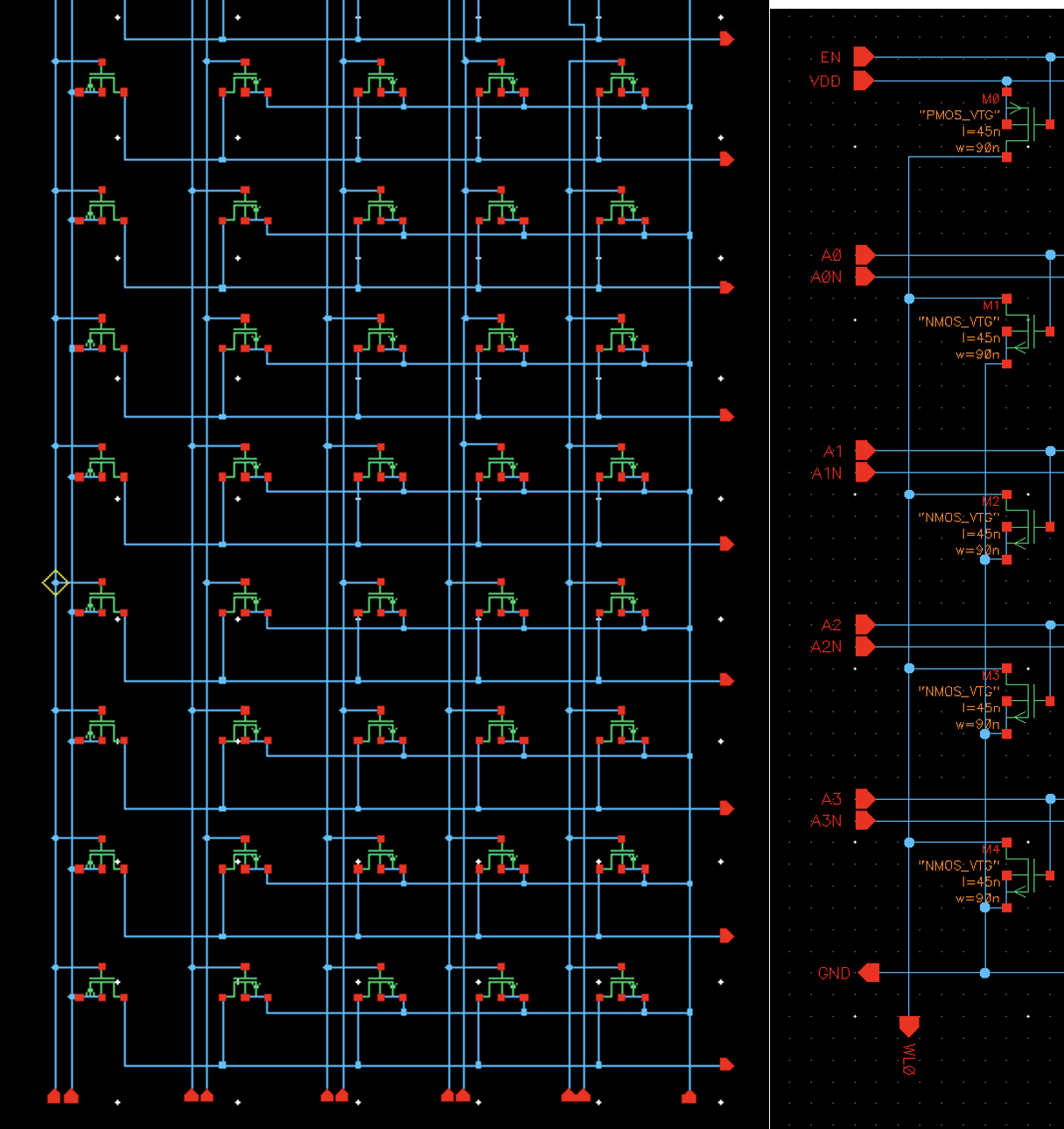
Memory System
The memory subsystem is fully custom and transistor-accurate.
It includes:
- a custom SRAM bitcell designed for stable storage and access
- a 16×4 NOR-based decoder used for memory addressing and control
These components were designed and validated independently, then integrated into the datapath.
Signal Conditioning
To support signal integrity and timing stability, the system includes a custom inverter chain used for buffering and propagation control across the datapath.
This helps manage loading effects and signal degradation between blocks.
Design Approach
This project followed a full-custom VLSI workflow:
- schematic capture in Cadence Virtuoso
- hierarchical block composition
- simulation-based validation
- functional verification
- structural system integration
All validation was performed at the schematic level using circuit simulation — not behavioral modeling.
Validation
All subsystems were verified through simulation, including:
- functional correctness
- signal stability
- decoder operation
- SRAM cell stability
- datapath behavior
Timing and validation results are documented in the final report.
Documentation
Final Report
Download Final Report (PDF)
Project Presentation
Download Presentation (PDF)
Context
Course: ECE 467 – Introduction to VLSI
Institution: University of Illinois Chicago
Term: Fall 2025
Tool: Cadence Virtuoso
Personal Impact
This was my first real transistor-level system design project - not abstract logic, not HDL, not blocks on a diagram. Actual devices, actual circuits, actual integration.
It taught me how digital systems are actually built:
- bottom-up from devices
- validated through simulation
- composed hierarchically
- and integrated into real architectures
This is the kind of foundation used in ASIC design, memory systems, and custom digital IC work, and it’s one of the projects that pushed me toward VLSI as a focus area.
Gallery
Click an image to open full size.